Samsung S6 Circuit Diagram
Galaxy s6 teardown: all about the galaxy s6 and s6 edge – samsung Samsung galaxy schematics s8 s9 pdf I9192 schematics i9500
[Get 33+] I9500 Schematic Diagram Download
[get 33+] i9500 schematic diagram download Samsung schematics & manual 24 galaxy s6 diagram
[get 30+] galaxy s6 schematic diagram download
Samsung galaxy s7 schematics mobile manual edge phone diagram motherboard circuit pdf service android diagrams inside schematic teardown parts mainSamsung pcb galaxy 4g board components layout motherboard ic power gsm solution management Galaxy schematics samsung s6 schematic diagram manual g920t pcb mobile g920a service s8Galaxy s schematics.
Samsung galaxy schematics s5 s6 mobileSamsung galaxy s 4g pcb board components layout Schematics edge j7 alisalerSamsung s6 edge sm-g925f charging solution.
![[Get 29+] Galaxy S6 Schematic Diagram Download](https://i2.wp.com/phonelumi.com/wp-content/uploads/2016/09/schematics-samsung-s7edge.jpg)
Schematics g935f
Schematic s8 schematicsOnv e99006 type s6 circuit board #1 Fault dunSchematics s6.
[get 29+] galaxy s6 schematic diagram downloadGalaxy s schematics Galaxy s schematicsSamsung s8 schematic pdf.
![[Get 29+] Galaxy S6 Schematic Diagram Download](https://i2.wp.com/lh3.googleusercontent.com/proxy/k0C-GY-RJlvBRz8EKHaPTW5oq_-iVZIuho0AlU2U0M3gA0_NpaMFi6cUN_z0_JGtxI9LgKrLiuPH_RkYYgFXBIAtfD-SLusuVb0FN6IAYujCAR8K2lQfExzb=w1200-h630-p-k-no-nu)
Samsung galaxy s9+ sm-g965f schematics
Board s6 onv circuit typeSchematics schematic g925 Teardown s6 amoledWiring lollipop touchwiz samsungs android.
[get 29+] galaxy s6 schematic diagram download[get 30+] galaxy s6 schematic diagram download 24 galaxy s6 diagramSamsung galaxy s7 power without battery.

S9 samsung galaxy schematics sm g965f plus
S7 dh indicate sensor aeG925f s6 charging .
.


24 Galaxy S6 Diagram - Wiring Diagram Niche
![[Get 30+] Galaxy S6 Schematic Diagram Download](https://i2.wp.com/lh6.googleusercontent.com/proxy/1cU6NTmnZ4LsWNCroh0Hh9V0kZq1QQqvNWF756rWqWbWCGO5NXqBnivDHUIfI9bAxa3pWojeF_amQRRatM4V-ZBETYf8pKQPi7IAKeaRj-syAPDyINyuFIODxMhZlI_E9_HzbBxuUYjHYQ=w1200-h630-p-k-no-nu)
[Get 30+] Galaxy S6 Schematic Diagram Download

Samsung Galaxy S9+ SM-G965F schematics
![[Get 30+] Galaxy S6 Schematic Diagram Download](https://i2.wp.com/image.jimcdn.com/app/cms/image/transf/dimension=820x10000:format=jpg/path/s9561acb0f0916d6e/image/ib44a18627c2e45ba/version/1552166040/samsung-galaxy-s3-schematics.jpg)
[Get 30+] Galaxy S6 Schematic Diagram Download

Samsung Schematics & Manual - All Keypad & Android Mobile circuit
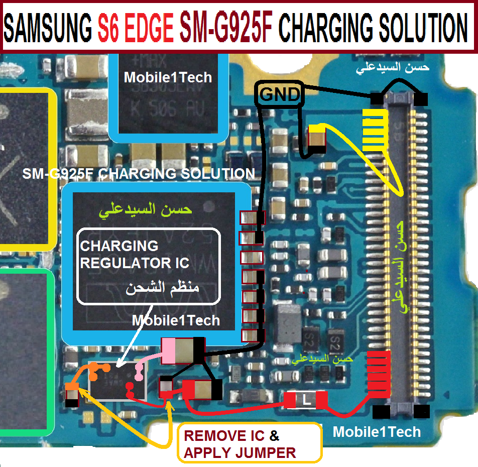
SAMSUNG S6 EDGE SM-G925F CHARGING SOLUTION

Samsung S8 Schematic PDF - Schematic Diagram
![[Get 33+] I9500 Schematic Diagram Download](https://i2.wp.com/phonelumi.com/wp-content/uploads/2016/10/samsung-galaxy-s4-i9192.png?x45285)
[Get 33+] I9500 Schematic Diagram Download